 Warning
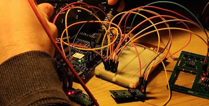
PCB-Design ist der Prozess der Übersetzung eines Schaltplans in ein physisches Board-Layout. Wir verwenden branchenübliche Werkzeuge, um Komponenten zu platzieren, Leiterbahnen zu routen und die Signalintegrität zu prüfen, bevor wir die Dateien zur Fertigung senden.
How to create electronics for your project?
Examples
Unser Prozess
Requirements & Specification
Define what the circuit needs to do — power budget, interfaces, environment, communication protocols, and any regulatory constraints (CE, FCC, RoHS).
Schematic Design
Translate the specification into a circuit schematic. Component selection, power regulation, signal chains, protection circuits, and connector pinouts are all resolved at this stage.
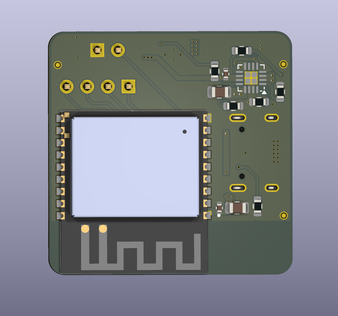
PCB Layout
Place components and route traces with signal integrity, EMC, and DFM in mind. We define layer stackup, controlled impedances, copper pours, and thermal management before release.
Design Review & Simulation
Run DRC, ERC, and thermal analysis. Critical sub-circuits are simulated in LTspice before the board is sent to fabrication to catch issues early.
Prototype & Bring-Up
Gerbers go to the fab, components are assembled, and the board is brought up incrementally using bench instruments — power supply, oscilloscope, logic analyser.
Testing & Validation
Functional tests against the original specification. We document test results and iterate on any issues before sign-off for production.
Production Files
You receive gerbers, BOM, pick-and-place files, test specification, and schematic PDF — everything your contract manufacturer needs to produce the board at scale.
Häufig gestellte Fragen
Können Sie eine Leiterplatte von Grund auf entwerfen?
Ja. Wir übernehmen den gesamten Prozess von der Anforderungsanalyse über das PCB-Layout bis zur Produktionsdateiübergabe.
Für welche Zertifizierungen legen Sie aus?
Wir entwickeln von Beginn an mit CE-, FCC- und RoHS-Konformität im Blick, unter Berücksichtigung von EMV und Signalintegrität.
Montieren und testen Sie die Leiterplatten auch?
Wir übernehmen Prototypenmontage und Inbetriebnahme im eigenen Haus. Für Produktionsmengen liefern wir ein vollständiges Paket (Gerber-Dateien, BOM, Pick-and-Place) für Ihren Auftragsfertiger.
Wie lange dauert das PCB-Design?
Eine typische 2–4-lagige Prototypenplatine dauert 2–4 Wochen von der Spezifikation bis zur Gerber-Freigabe. Komplexere Designs dauern länger.
Welche Designdateien liefern Sie?
Sie erhalten Gerber-Dateien, Schaltplan-PDF, BOM, Pick-and-Place-Datei und eine Testspezifikation — alles, was ein Auftragsfertiger benötigt.